

EMC-TA On Track: Electromagnetic noise under control
Fernando Arteche (ITAINNOVA), 27/05/2016
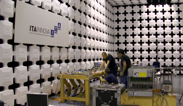
Interior of the SVD test chamber at the EMClab at ITAINNOVA (Image: ITAINNOVA)
For detector designers, electromagnetic noise is one of the biggest factors to take into consideration. Noise levels define the minimum signal that detector electronics can process, which impacts its sensitivity.
High magnetic fields, large amounts of cables, highly sensitive electronics, and the proximity of potential interference sources to sensitive modules pose problems in the design of the next generation of detectors.
If only addressed during test-beam campaigns and detector commissioning, successful detector integration could be extremely difficult due to the complexity of the system and electromagnetic noise environment. This added complexity makes the identification of noise sources, noise victims and coupling mechanism challenging.
As such, efforts to control these problems require special facilities free of electromagnetic ambient noise and proper equipment as well as specific detector know-how to carry out Electromagnetic Compatibility (EMC) tests and characterizations.
Via the AIDA-2020 project, the physics community now has access for the first time to an EMC laboratory specially focused on EMC tests for electronic noise characterization and grounding diagnostics at the Instituto Tecnológico de Aragón (ITAINNOVA) in Spain. The resulting noise studies will allow front-end electronics (FEE) to enhance their interference immunity in order to assess compatibility with the noise generated by the power supplies, transmitters or any other interference source present in the detector.
The ITAINNOVA facility has already been used for this purpose during the first year of the AIDA-2020 project. A group of researchers from the Institute of High Energy Physics (HEPHY) at the Austrian Academy of Sciences (responsible for the design of the readout system of the Silicon Vertex Detector (SVD) for the Belle II experiment at the KEK laboratory in Japan) spent two weeks at ITAINNOVA performing a full EMC characterization of one prototype of the SVD detector.
After the SVD system showed poor performance due to electromagnetic noise during a test beam campaign in 2014, the HEPHY group requested a full EMC characterization of the SVD system at ITAINNOVA. This would allow the group to improve the design and make the system more robust to noise interference. During their two week stay, HEPHY members collaborated with ITAINNOVA staff to conduct transient, interference and noise emission tests of the power supplies, as well as noise susceptibility tests of the FEE.
The most revealing test of their stay was the injection noise to the FEE to evaluate the susceptibility of a mid-scale prototype of the SVD system to ground interference currents. This test identified weak points in the design, such as sensitive connections and frequencies. Dr. Markus Friedl of the HEPHY group commented: “The outcome of this test campaign shows that SVD needs to change several system design aspects in order to ensure the correct integration of modules, hybrids, FEE and power units.”
The main advantage of this test is that the chamber operates as an “electromagnetic clean room” which allows to keep the noise floor present in the system very low (below 500nA in a wide frequency range). This test campaign has provided an evaluation of the SVD FEE grounding topology; power supplies specifications and SVD FEE susceptibility to conducted noise currents and transients.
The knowledge gained from the test allowed the HEPHY group to set new EMC design rules and specifications for power units for the SVD. Quite recently, this new design has been implemented and tested during a new test beam at DESY (Hamburg, Germany) with big success.