

Versatile TSVs for science and industry
Jennifer Toes (CERN), 11/12/2017
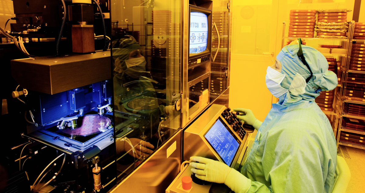
A clean room technician completing a lithography process step on one ATLAS TSV wafer (Image: Fraunhofer IZM)
In early 2017, AIDA-2020 announced it had selected a project led by the University of Bonn, in partnership with Fraunhofer IZM, to receive support from the AIDA-2020 Proof-of-Concept (PoC) fund.
The fund aims to develop industry-oriented and innovative projects based on detector science and technology with broader applications outside of the field. The CERN Knowledge Transfer Group coordinates the fund within the remit of AIDA-2020 Work Package 2, dedicated to innovation and outreach.
The Bonn-IZM pixel project focuses on the development of ‘Advanced Through Silicon Vias (TSVs) for pixel detectors’, with a focus on standardising the TSV processes. If successful, industrial partners, especially small and medium companies, will have access to a more affordable and, therefore, competitive option. TSVs offer high-density vertical stacking of microchips used in electronics, providing a smaller and simpler structure, whilst increasing connectivity and performance. TSVs are currently used across many industries, and can be found in technologies such as memory chips and interposers.
In high-energy physics research, scientists can make use of TSVs in the design of new detector components. However, many TSVs are often highly specialised for industry, making their processes less suitable or even unavailable for use in other fields.
To be useful in the design of advanced hybrid pixel detectors, the TSV process needs to be compatible with niche requirements and technology, such as fine pitch, high-density bump, and flip-chip bonding.
As such, the TSV project selected for the AIDA-2020 PoC fund aims to demonstrate the technological feasibility of this kind of interconnection for use in pixel detectors for charged particle tracking. In particular, the project researchers will focus on developing a versatile via-last TSV process with pixel detector readout wafers for the ATLAS experiment based at the Large Hadron Collider at CERN in Switzerland.
Fabian Hügging, senior scientist at the University of Bonn and leader of the Bonn-IZM TSV project, said “We hope to demonstrate the feasibility of a versatile via-last TSV process used on standard ASIC wafers fabricated in modern CMOS technologies. We want to develop a compact hybrid pixel detector module which can be operated entirely via the back side of the readout chip through the TSV.”
Currently the TSV formation process and the fabrication of the redistribution layers on the back end of the chips are improved towards high yields while keeping the fine-pitch bump bonding to the pixel detector sensor chip.
Once optimized, the TSV process will make the technology available for various functions and projects, allowing a more standardised process for partners across both academia and industry. Indeed, the new, versatile TSVs will have applications with imaging sensors, heterogeneous integration, and hermetic capping of sensitive sensor components; which may be of use in packaging processes, X-ray imaging, and both industrial and commercial cameras. The work kicked off in spring 2017 at Bonn, where the collaborators agreed upon the project implementation plan and delegation of tasks. The project work is divided into five Work Packages, each dedicated to specific technological tasks, such as optimising the wafer design, bonding process, and chip sensor assemblies.
The project aims to achieve its goals prior to the completion of the AIDA-2020 project in 2019.