

New Irradiation Facility in Slovenia
Vladimir Cindro (Jozef Stefan Institute, Slovenia), 16/01/2018
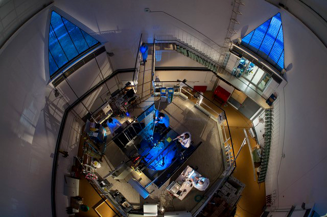
Top view of the reactor water tank. Fuel elements are on the bottom, blue Cherenkov light is emmited by charged particles moving faster than light in water. (Image: Branko Čeak, National Geographic, Slovenia)
Radiation hardness is a key issue for components installed in collider experiments. Therefore many irradiation studies have been performed in the past 20 years at the TRIGA reactor at the Jozef Stefan Institute (JSI) in Slovenia. An increase in the need to irradiate larger components inspired the construction of a large object irradiation facility in the framework of AIDA-2020. In 2016, the facility was designed, manufactured and installed in the Tangential Channel of the JSI TRIGA reactor, a horizontal channel piercing the concrete biological shield, the reactor tank and the graphite reflector around the core.
Before the new channel was built, objects were irradiated in reactor core. The new facility allows users to make irradiations of objects with lateral dimensions of up to 12 cm in a relatively intense neutron flux, of the order of 1012 cm-2s-1.
The new irradiation device provides easy insertion and withdrawal of samples, online irradiation testing of electronic components, and shielding from neutron and gamma radiation originating from the reactor core. The irradiation device also ensures protection of the interior components of the Tangential Channel, especially the water-tight stainless steel manifolds which join sections of the channel located inside the reactor tank.
In November 2017, a group of researchers from DESY, working on the ATLAS experiment at CERN, became the first external users to perform first irradiations in the new channel. The tests were carried out with the help of the AIDA-2020 Transnational Access programme.
For the ATLAS Phase-II Upgrade, the current inner detector will be completely replaced. The new ATLAS tracker will be composed of silicon pixel and strip modules. These modules consist of a silicon sensor and a readout flex board, which is glued on the top of the sensor. As the sensor cools down, it can undergo mechanical stress due to thermal expansion. The stress on the sensor leads to changes in leakage currents, surface resistances and might cause micro cracks, which increases the probability of electrical breakdown.
Radiation-induced damage inside the silicon lattice could increase the probability of micro cracks as well as increasing the piezoelectrical effects on the electrical properties of the sensor. Therefore, it was necessary to evaluate the changes of the electrical properties of silicon sensors under mechanical stress before and after irradiation and to estimate the risk of cracks caused by mechanical stress.
The DESY user group asked for irradiations of 25 silicon wafers of 100 mm in diameter. The wafers were irradiated to 2 1015 ncm-2 in a new channel. Irradiation itself takes about two hours, but sensors may only be removed from the reactor after 24 hours, due to activation of material.
Following this, three further projects for irradiation in the tangential channels are underway, where researchers will irradiate: electronic boards for the ATLAS tile calorimeter, full-size ATLAS sensors for the new inner tracker, and hexagonal silicon sensors fabricated on 6-inch wafers for the CMS calorimeter.